
Alphabet’s AI buildout stopped looking like a planning assumption and started looking like a 2026 procurement event when the company lifted full-year capital expenditure guidance to $195–205 billion, up from $175–185 billion, after spending $44.9 billion in Q2 alone. The financing signal was just as blunt: Alphabet completed its first equity raise since 2004, bringing in $49.6 billion in June 2026, and added roughly $84 billion in debt, taking total debt to about $100 billion from roughly $16 billion. CFO Anat Ashkenazi also said Google would “expand the use of third-party capacity in Q3 as a bridging strategy,” which is the kind of sentence procurement teams hear differently than investors do. It means internal deployment capacity is not the only governor on the plan.[1]
That is the right entry point for Alphabet’s 2026 AI infrastructure supply chain. The issue is not whether Alphabet is spending on AI. It is where that spending becomes physically hard to redirect once wafers, HBM, optical switching, substrates, ODM slots, power equipment, and cooling capacity are spoken for.
For scale, Goldman Sachs projected more than $690 billion of hyperscaler AI capex in 2026, so Alphabet is not operating in an empty lane. Its suppliers are being asked to allocate against several large buyers at once, and Alphabet’s own increase is large enough to change supplier behavior before every dollar has turned into recognized revenue.[2]

The Six-Layer Map Behind The Capex Number
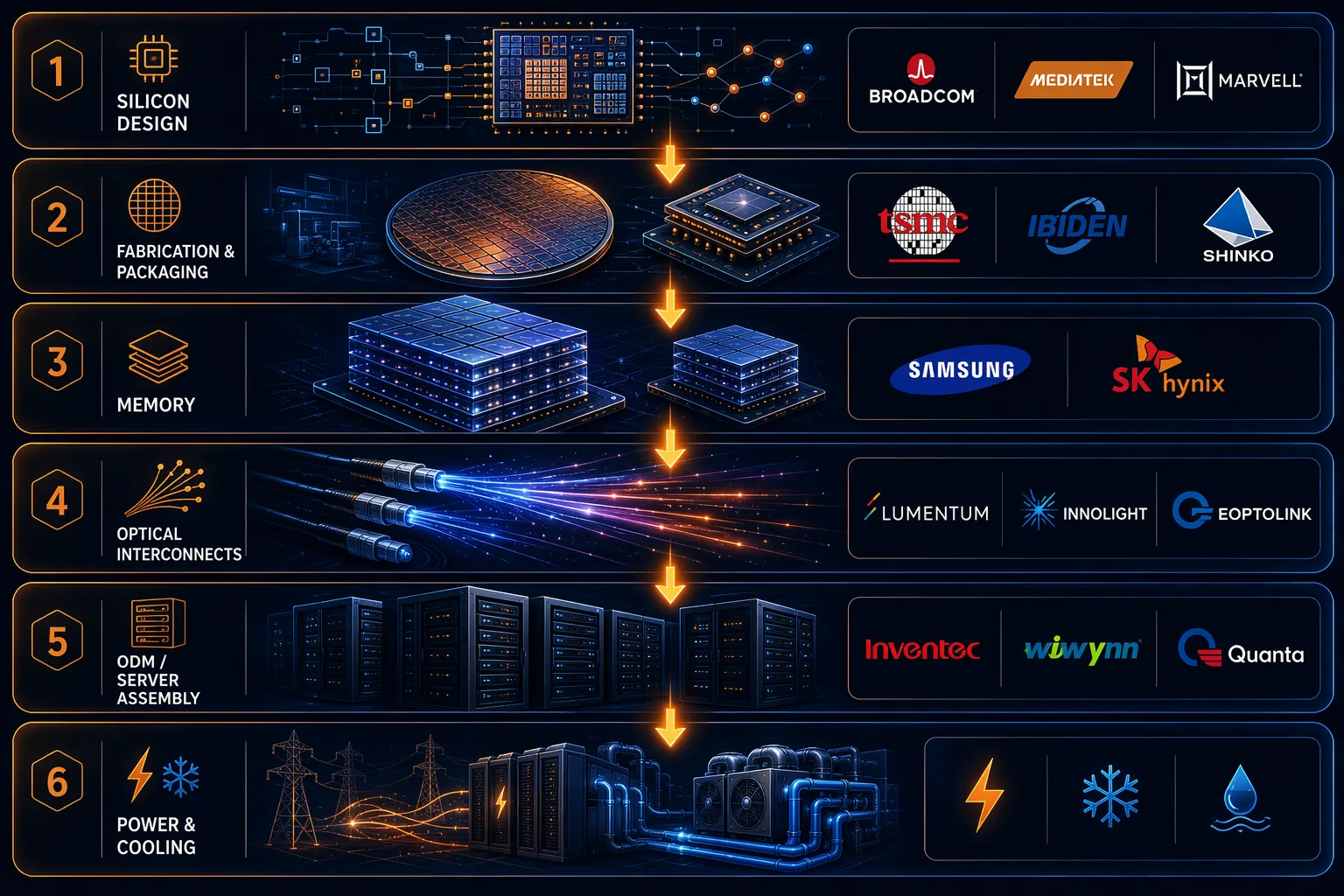
Data Gravity’s TPU supply chain map is useful because it refuses to compress Alphabet’s AI infrastructure into a chip-vendor list. It identifies at least 15 vendors across six layers: silicon design, fabrication and packaging, memory, optical interconnects, ODM and server assembly, and power and cooling infrastructure.[3] That is closer to how sourcing teams experience the buildout: not as one contract, but as a stack of interlocked allocations.
| Layer | Vendors And Inputs Identified In The Research | Why Procurement Should Care |
|---|---|---|
| Silicon design | Broadcom, MediaTek, Marvell; Intel around surrounding Xeon and IPU infrastructure | Design partnerships determine qualification paths, software integration, board design, and future negotiating leverage. |
| Fabrication and packaging | TSMC N3P/N2; CoWoS advanced packaging; Ibiden and Shinko packaging substrates | Even a diversified chip-design strategy can converge on the same wafer and advanced-packaging bottleneck. |
| Memory | Samsung and SK Hynix HBM | HBM allocation affects accelerator availability, power-performance economics, and the ability to ramp specific TPU generations. |
| Optical interconnects | Lumentum, Innolight, Eoptolink | Optical switching can change pod-level power requirements and deployment architecture, not just component cost. |
| ODM and server assembly | Inventec, Wiwynn, Quanta | Server integration capacity determines how quickly accelerators become deployable infrastructure. |
| Power and cooling | Power ICs, grid and generation equipment, cooling infrastructure, helium and related upstream inputs | Facility-side constraints can delay deployment even when compute hardware is available. |
The table is deliberately uneven. Some positions are replaceable with pain. Others require redesign, requalification, or a change in deployment architecture. That distinction matters more than vendor count.
Silicon Design Is Diversifying, But Not Escaping Physics
Google’s custom-chip strategy is broader than the public conversation around one TPU partner suggests. TNW described a four-partner strategy in which Broadcom supports training-focused custom silicon, MediaTek is tied by supply-chain reporting to a cost-optimized inference chip at an estimated 20–30% lower cost, Marvell is described as being in negotiations around memory processing units, and Intel remains relevant around surrounding Xeon and IPU infrastructure.[4]
The important caveat is that not all of these relationships carry the same confirmation level. Broadcom’s position is the most visible and mature. MediaTek’s reported “Zebrafish” work at TSMC 2nm and Marvell’s role should be treated as supply-chain-reported or negotiation-stage material, not as fully confirmed Google roadmap disclosures.[4]
That still makes the strategy rational. Alphabet is trying to avoid overconcentration at the chip-design layer by using different partners for different accelerator and infrastructure functions. The problem is that design diversity does not automatically produce manufacturing diversity. If the resulting custom silicon still depends on TSMC advanced nodes and CoWoS packaging, the sourcing map narrows again at the point where capacity is scarcest.
Broadcom: The Locked Custom-ASIC Position
Broadcom is not merely “exposed” to Alphabet’s AI spending. It is structurally embedded. The research brief identifies Broadcom as locked into the relationship through 2031, with a $73 billion AI backlog and more than 70% of the custom AI accelerator market. Mizuho estimates Broadcom AI revenue of $21 billion in 2026, rising to $42 billion in 2027.[5]
That combination changes the replacement math. A procurement team can dual-source many commodities by accepting price or lead-time tradeoffs. Replacing a custom ASIC partner means reopening design, validation, firmware, board, thermal, and manufacturing assumptions. It also means asking a different supplier to absorb volume while the rest of the industry is competing for the same advanced-node and packaging capacity.
Broadcom’s leverage is therefore not just contractual. It sits in accumulated design knowledge and qualification history. Alphabet can and does cultivate alternatives, but a second or third design partner does not instantly become a substitute for an already-ramped custom accelerator program.
Samsung: HBM Allocation As A Deployment Constraint
Samsung’s importance comes from a different source: memory allocation. The research brief identifies Samsung as supplying roughly 60% of HBM3E for Google’s Ironwood TPU. It also notes that all 2026 HBM production had been allocated before the year began, with mid-teen to low-twenties percentage price increases.[6]
That is not a generic memory shortage claim. In an accelerator build, HBM is tied to performance, power, package design, and ramp timing. If the HBM allocation slips, the accelerator does not simply ship with a cheaper substitute. The package, qualification process, and supply agreement have already narrowed the path.
SK Hynix remains part of the mapped memory layer, and Alphabet is not dependent on a single HBM vendor in the broadest sense.[3] But the Ironwood-specific allocation makes Samsung more than one logo in a dual-source strategy. It is the supplier whose allocated volume can determine how much of a TPU generation becomes deployable in the intended window.
Lumentum: A Sole-Source Optical Component With Architectural Weight
Lumentum is the easiest supplier to underestimate if the map is read as a semiconductor screen. The research identifies Lumentum as the sole-source supplier of Google’s Apollo Optical Circuit Switch, with deployment of 12,000–15,000 units in 2026. The same material says Apollo cuts power by 95% compared with electronic switching, at roughly 100W versus about 3,000W per pod.[7]
That power delta is not a rounding error in a constrained data center. It affects electrical design, cooling load, pod architecture, and the number of deployable clusters inside a facility envelope. When a component changes the deployment architecture this much, sole-source status becomes more serious than ordinary supplier concentration.
Innolight and Eoptolink still matter in the optical interconnect layer.[3] But Apollo is the point where the supplier relationship hardens. Substituting a transceiver supplier is one kind of sourcing problem. Substituting the sole-source component behind a lower-power optical switching architecture is a different one.

The CoWoS Tension Under The Multi-Vendor Strategy
The clean version of Alphabet’s strategy is multi-partner: Broadcom, MediaTek, Marvell, Intel, Samsung, SK Hynix, Lumentum, Innolight, Eoptolink, Inventec, Wiwynn, Quanta, and the fabrication and substrate vendors around TSMC, Ibiden, and Shinko. The messier procurement version is that multiple lanes still converge on advanced manufacturing and packaging.
TrendForce and DigiTimes-related estimates put 2026 TPU shipments in a wide range: about 3.3 million in a CoWoS-constrained view and about 4.6 million in a Bank of America estimate. The spread should not be treated as simple forecasting noise. It points to real uncertainty around how much advanced packaging capacity Alphabet can secure.[8]
The same research context forecasts custom ASIC servers growing 64.2% versus 43.8% for GPU servers.[8] That matters because Alphabet is not the only customer trying to move more AI compute into custom silicon. A shift toward custom ASIC servers can relieve one form of dependency while intensifying pressure on the packaging, substrate, and memory stack those ASICs require.
This is why the CFO’s third-party capacity bridge matters. It is a signal that the bottleneck is not isolated to chip design or internal data center construction. Alphabet can design more paths, but the deployment calendar still has to pass through suppliers that cannot be expanded by management intent alone.[1]
Shortage Inputs Sit Below The Named Vendors
The named-vendor map is still not the whole supply chain. Fusion Worldwide’s Q1 2026 State of the Industry report, summarized by Supply Chain Connect, described an eight-category simultaneous shortage environment affecting inputs such as helium, T-glass substrates, ABF film, power ICs, and related materials.[9]
These are not glamorous dependencies, but they are exactly the kind that turn a supplier strategy into an allocation problem. T-glass and ABF film sit under advanced packages and server boards. Power ICs sit under the systems that make accelerators usable. Helium disruptions can reach semiconductor manufacturing and cooling-related processes. The research brief notes that the helium disruption tied to Iranian strikes on Qatar’s Ras Laffan was current as of Q1 2026, so it should be monitored as a live geopolitical constraint rather than treated as a permanent condition.[9]
For a broader bottleneck framework, the adjacent problem is covered in why AI data centers face five supply chain bottlenecks. Alphabet’s case is narrower and more urgent: the capex is already guided, the supplier map is already taking shape, and the constraint set is moving from abstract scarcity to allocation decisions.
ODM Capacity Converts Components Into Deployable Infrastructure
Inventec, Wiwynn, and Quanta appear in the mapped ODM and server assembly layer.[3] They do not get the same attention as accelerator or HBM suppliers, but their role is where purchased components become shippable, rackable systems. If server integration capacity tightens, an available chip is still not an available cluster.
This is also where procurement teams should be careful with the phrase “multi-vendor.” Multiple ODMs can reduce exposure to any one assembler, but they may still depend on the same accelerator schedule, HBM allocation, substrates, NICs, optics, power components, and facility readiness. A second assembler does not solve a missing package substrate.
Server economics are their own constraint layer; readers tracking that angle can compare the ODM pressure with Supermicro’s AI server margin dynamics. The immediate Alphabet question is simpler: which assembly partners have enough slots, qualified processes, and component visibility to absorb a ramp of this size?
Power And Cooling Are Not Afterthoughts
The power and cooling layer is where the infrastructure plan meets the utility calendar. Alphabet’s procurement exposure does not end when the server ships. Transformers, switchgear, backup power, cooling systems, grid interconnection, and power generation equipment determine whether capacity can be energized on the timeline implied by the capex plan.
That is why optical switching and facility power should be read together. Lumentum’s Apollo role matters partly because lower switching power gives Alphabet more room inside a constrained energy and cooling envelope.[7] On the supply side, power infrastructure bottlenecks increasingly have their own supplier concentration profile; the GE Vernova case is one example of how generation and grid equipment can become the pacing item for AI infrastructure deployment.
Readers focused on that layer can use GE Vernova’s AI infrastructure bottleneck as the next supplier-specific lens. Alphabet’s $195–205 billion guidance makes the point immediate: power equipment is not a downstream facilities issue if it controls when compute capacity turns on.[1]
What Procurement Teams Should Watch
The useful watchlist is not a list of every company touching Alphabet’s capex. It is a list of points where substitution becomes expensive under time pressure.
- Broadcom design-lock evidence: backlog conversion, confirmed TPU-related program duration, and any signs that alternative ASIC partners are taking over qualified production rather than future exploratory work.
- Samsung HBM allocation: Ironwood TPU memory mix, 2026 and 2027 allocation commitments, price changes, and whether SK Hynix gains a larger practical share in specific TPU generations.
- Lumentum Apollo deployment: unit volumes, sole-source status, optical switch qualification alternatives, and whether the power advantage remains large enough to preserve architectural dependence.
- TSMC CoWoS capacity: the gap between lower and higher TPU shipment estimates, substrate availability at Ibiden and Shinko, and whether any packaging constraint delays custom ASIC servers.
- Third-party capacity usage: how long Alphabet relies on external capacity as a bridge and whether that bridge competes for the same power, networking, and server supply base.
- Power and cooling lead times: grid equipment, power ICs, cooling systems, and facility readiness, especially where lower-power optical architectures affect deployment density.
Investment readers may connect this map to broader conviction around Alphabet’s AI cycle, including Berkshire’s Alphabet position and AI supply chain stocks. The procurement read is narrower. Alphabet’s supply chain is broad, but it is not evenly distributed. Many vendors participate. A few are structurally embedded. The signal to watch is not how many suppliers Alphabet names, but how many can be replaced when capacity is already under stress.
References
- Alphabet Q2 2026 earnings coverage, TechCrunch and Senanni Substack, 2026, TechCrunch / Senanni Substack
- Hyperscaler AI capex forecast, Goldman Sachs, 2026, Goldman Sachs
- 15-vendor TPU supply chain map, Data Gravity, 2026, datagravity.dev
- Google’s four-partner chip strategy, TNW, 2026, TNW
- Broadcom AI revenue and custom accelerator estimates, Mizuho, 2026, Mizuho
- HBM allocation and pricing research, TrendForce and DigiTimes, 2026, TrendForce / DigiTimes
- Apollo Optical Circuit Switch deployment and power data, Data Gravity, 2026, datagravity.dev
- TPU shipment estimates and custom ASIC server growth forecast, TrendForce and DigiTimes, 2026, TrendForce / DigiTimes
- Q1 2026 State of the Industry report, Fusion Worldwide via Supply Chain Connect, 2026, Supply Chain Connect
Comments
Join the discussion with an anonymous comment.